Shift Register - 74HC595
Shift Register
Suppose you’re working with an FND (Flexible Numeric Display). Even displaying a single digit requires 8 pins.
In cases like this, you can use a shift register to control 8 outputs with a single pin (at the cost of a small delay).
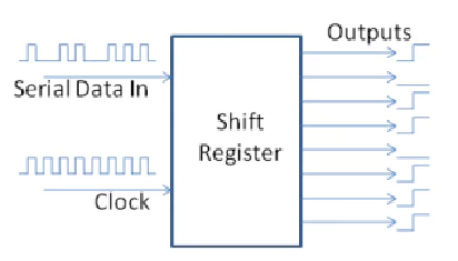
74HC595
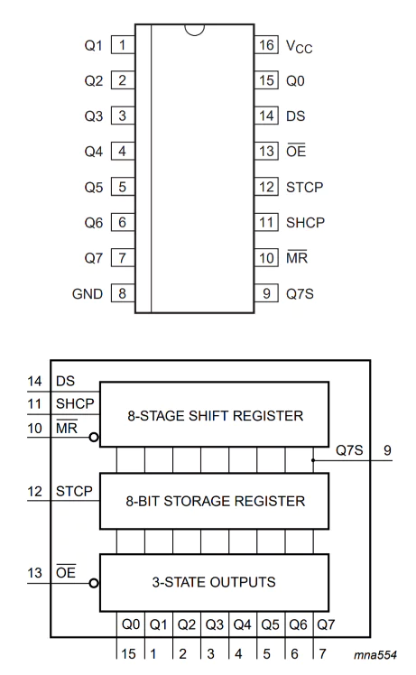
Q0 ~ Q7 : parallel output pins of register
DS : Serial data input pin
SHCP : shift register clock pin
STCP : storage register (Latch) clock pin
OE : output enable, can turn off the Latch’s output.
MR : master re-clear, can reset the shift register.
The shift register’s value isn’t output directly to Q0 ~ Q7.
There’s a Latch, and when the Latch clock rises, the value stored in the shift register is output to Q0 ~ Q7.
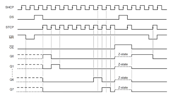 TIMING DIAGRAM
The control code flow is as follows:
Input a value on DS
A rising edge occurs on SHCP = the value shifts into the shift register
A rising edge occurs on STCP at the intended timing
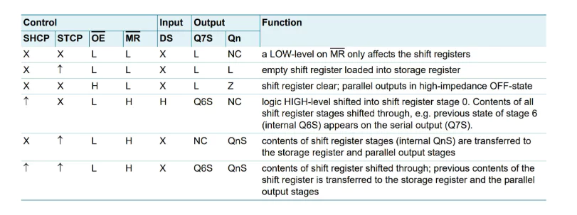 FUNCTION TABLE